Hardware
System Overview and Rack Setup
Below is a recommended configuration in comparison to a common SuperDARN system, Note that the N200s are in custom made shelves, but shelves can also be purchased from National Instruments:


Here is an actual rack configuration as installed by SuperDARN Canada at the Saskatoon (SAS) SuperDARN site. Note that space has been allowed between the rackmount items to allow for cable routing. There is a lot of cabling involved at the front of the devices.
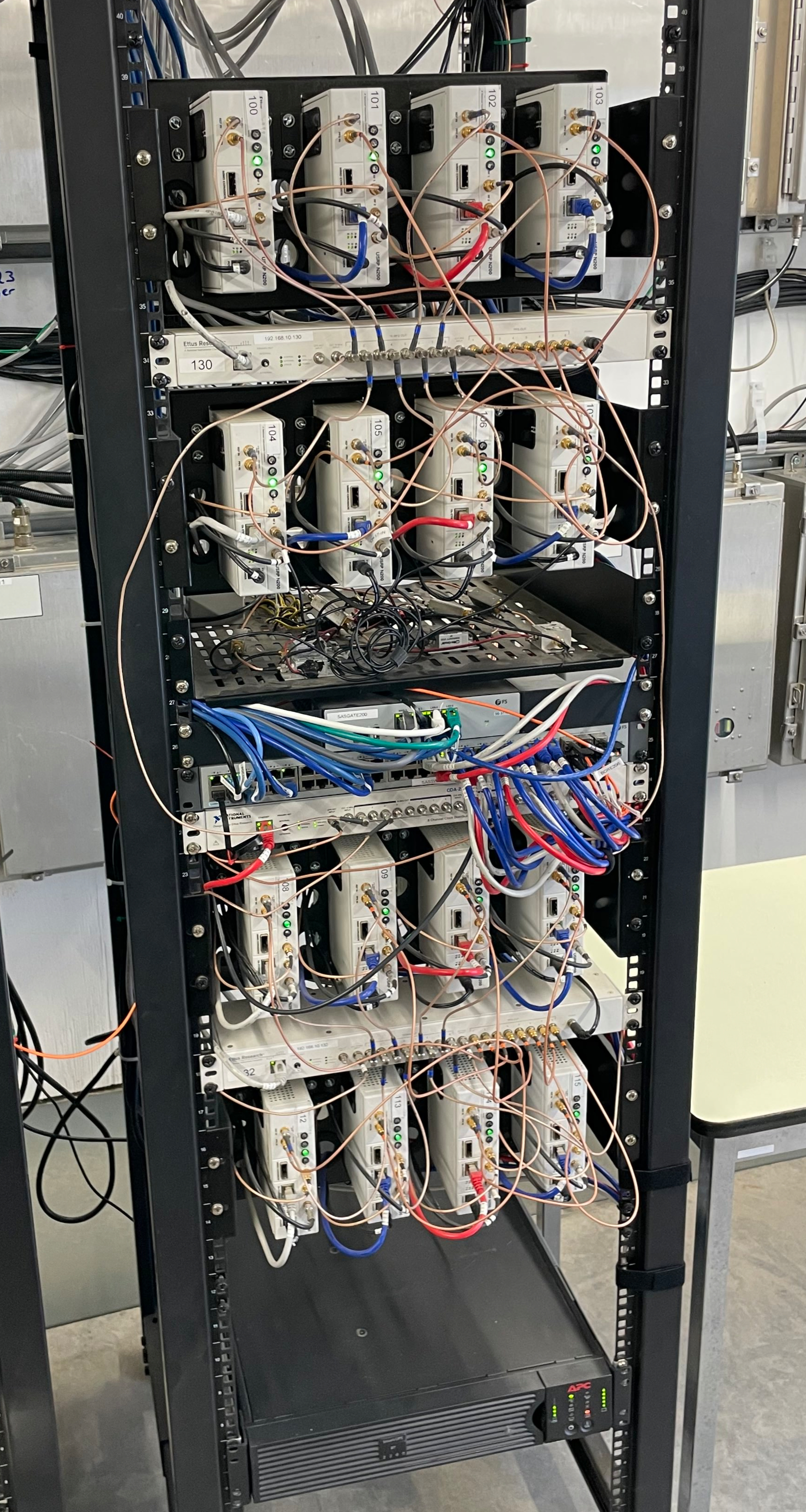
The items installed in the rack at the Saskatoon site are listed below in order from top to bottom in the rack:
USRP rackmount shelf (in-house design) with 4 x N200s
Ettus OctoClock
USRP rackmount shelf (in-house design) with 4 x N200s
Rackmount shelf with 4 x low-noise amplifiers for the interferometer receive channels, and a terminal strip for power (supplied by 15V Acopian power supply)
FS SG-3110 Dual WAN Security Gateway
FS S3900 48 Port 1GbE Switch
Ettus OctoClock-G (with GPSDO)
USRP rackmount shelf (in-house design) with 4 x N200s
Ettus OctoClock
USRP rackmount shelf (in-house design) with 4 x N200s
APC Smart-UPS X 2200 with AP6941 network card
In addition to these items, there are the following:
3 x AP7900B APC Power Distribution Units (PDUs) mounted at the back of the rack
4 x Tripp Lite power outlet strips mounted at the back of the rack
The Borealis computer is not in a rackmount case, instead it is placed to the right of the rack.
16 x Mini-Circuits SLP-21.4 low pass filters on the TX outputs of each N200
Synology Network Attached Storage (NAS) device
USRPs
This guide assumes set up of a brand new, unopened Ettus N200.
Initial Test of the Unit
Install Daughterboards
Open the unit and install the LFTX and LFRX daughtercards using hardware provided. The main USRP PCB is clearly marked with where to connect TX and RX daughterboards, and there is only one way they can fit while still allowing all the screw holes to line-up. The RX daughterboard is located directly above the fan power connection at the back of the motherboard.
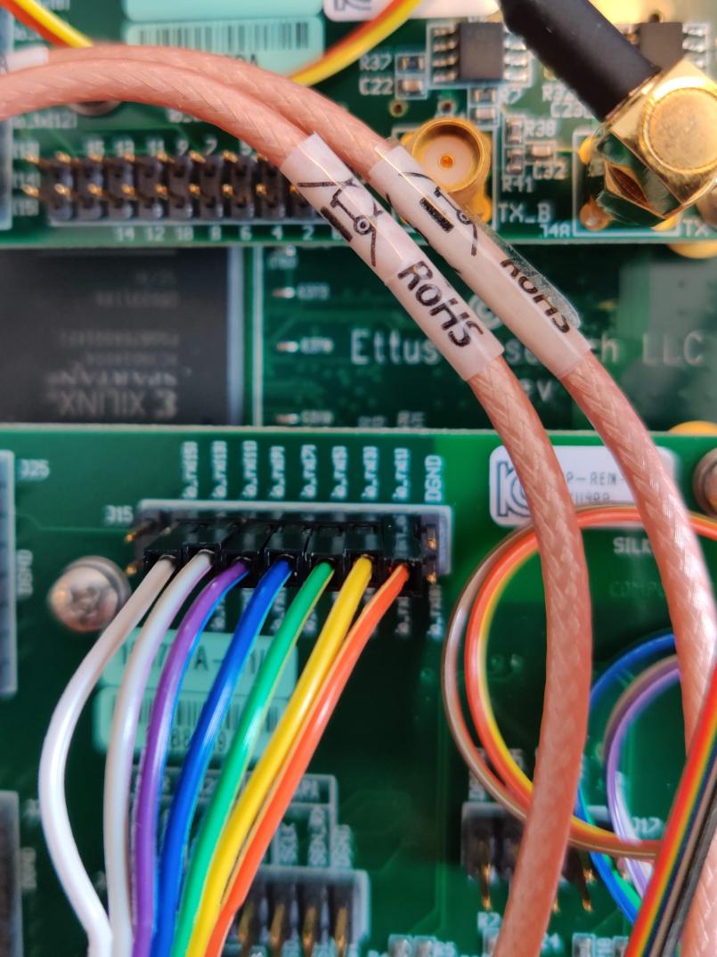
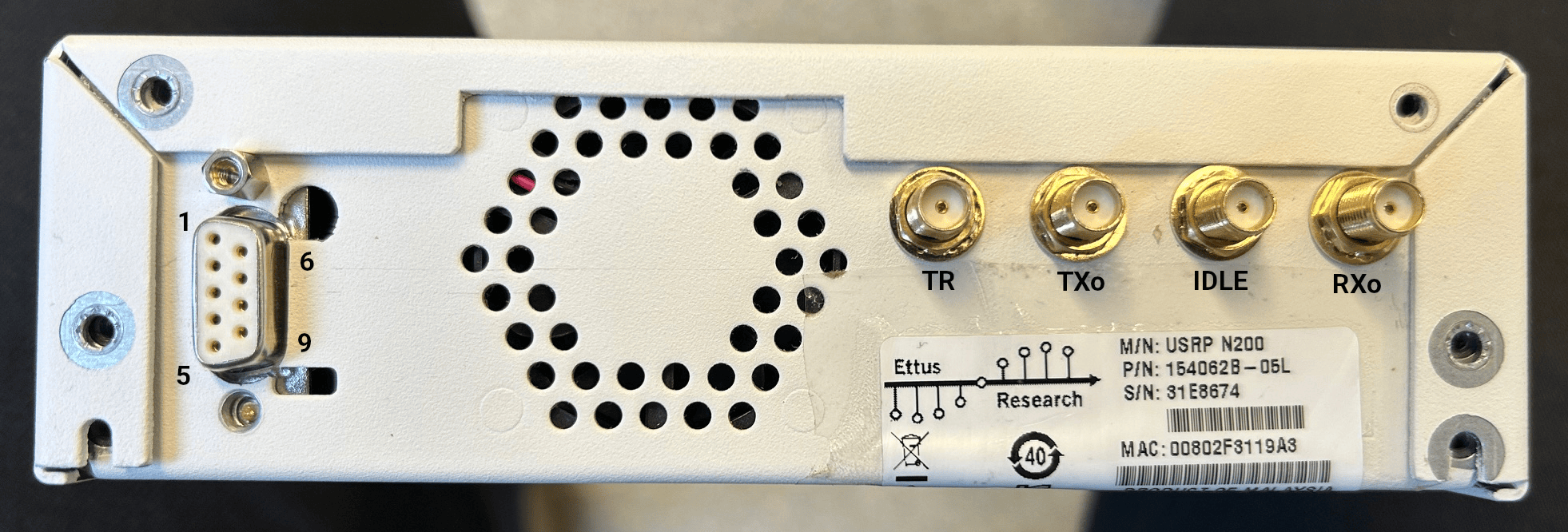
Connect the output of TXA using an SMA cable to the custom-added SMA connection point on the front of the USRP using one of the SMA Male to female bulkhead SMA cables. Connect the output of RXA to RF1 and RXB to RF2 on the front of the USRP using two more SMA Male to female bulkhead cables.
Verify that the jumper J510 on the N200 motherboard is jumping the two 0.1” header pins furthest from the board edge. The jumper is located behind the CLK_REF (REF IN) SMA connector on the front of the N200. This ensures that the reference clock input is coming from the front-panel SMA connector, and not the secondary SMA connector located on the motherboard labeled ‘J507 CLK_REF 2’.
Connect to the USRP
USRPs have a default IP address of
192.168.10.2. Assign a computer network interface an address that can communicate in this subnet. Connect the USRP to the computer’s network interface either directly or through one of the switches from the system specifications. Connect the USRP power supply.Note
If you have multiple N200s connected at once on the same subnet with the same IP address, the behaviour is undefined, and weird problems will result.
Verify the board powers on and is discoverable. The USRP should be discoverable by pinging
192.168.10.2. Ettus’ USRP UHD library supplies a tool calleduhd_usrp_probewhich should also be able to detect the device. See software setup for notes on installing UHD. The USRP may require a firmware upgrade.In order to do loopback testing, and see the transmit waveform on an oscilloscope with the N200: Connect an SMA T connection (F-M-F) to the TX output from the front of the N200, connect another SMA T (F-M-F) to the first T. Connect one end of the second SMA T to RX1, and the other end to RX2 with phase matched SMA M-M cables. Connect the free SMA output of the first SMA T to the scope. Connect the Octoclock PPS and 10MHz reference signals to the USRP. Make sure that the jumper on J510 is in the rightmost position connecting the front panel 10MHz as the system reference.
Test the USRP
Use the UHD utilities rx_samples_to_file, tx_bursts and txrx_loopback_to_file to
verify the USRP works. Use the scope to see the transmit signal. The RX samples will be a binary
file that can be quickly read in a plotted with Numpy/Matplotlib. While testing, watch the front
panel LEDs to see that they work as expected.
Disassembly for Enclosure Modifications
If the USRP is working correctly, the inner motherboard, fan, daughtercards and RF cables can all be removed from the unit. Carefully peel the product sticker and store with the motherboard, this contains the MAC address, SN and PN of the unit. All removed components and the sticker can be stored in the anti-static bags that were supplied with the unit. The enclosure is ready for machining the additional holes. Ensure that you note which way the fan was installed for reinstallation later.
Custom Enclosure Modifications
Machining Steps
Five extra SMA holes that are ‘D’ shaped to fit most standard SMA bulkhead connectors. Four of these holes are on the back of the N200, and one is on the front, in line with the two existing RF1 and RF2 SMA bulkhead holes.
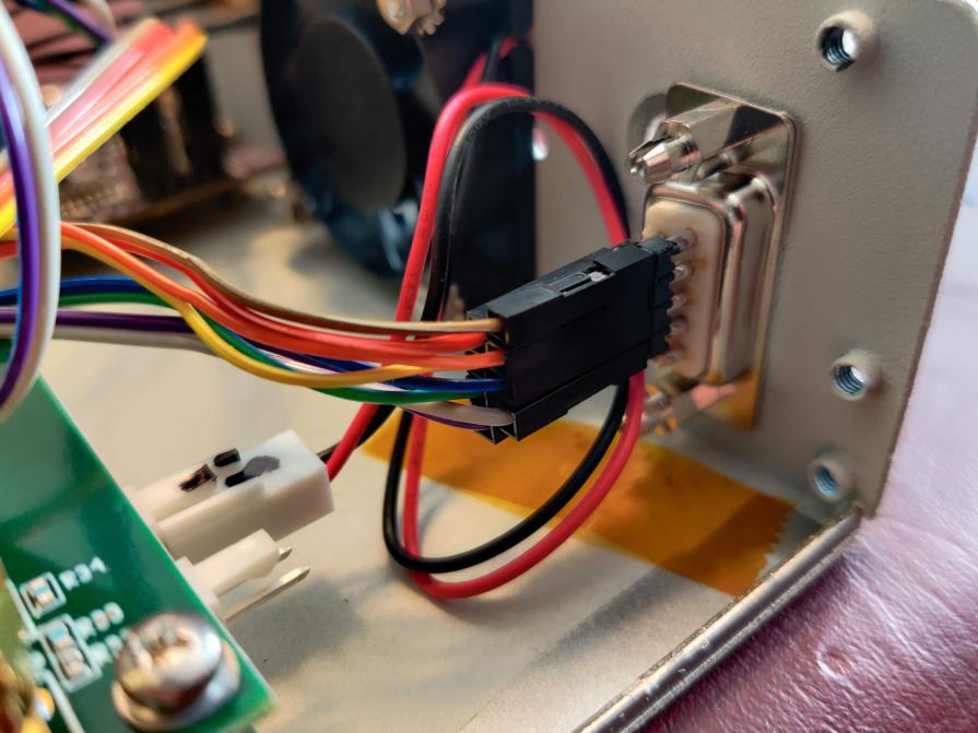
A DSUB shaped hole for a DE9 connector at the rear of the unit for connection to existing SuperDARN transmitters.
Four holes for standard 5mm LED clips (6.35 +/-0.05mm diameter) with 9.5mm centers to appropriately space them.
Installing the Custom-Made TXIO Board
Once the enclosures are machined, the electronics and components can all be reinstalled. Place the product sticker back in place on the rear of the unit. There are slight indentations in the case to indicate where the product sticker goes. Connect RXA to port RF1, connect RXB to port RF2, and connect TXA to the additional front panel hole that was added.
Install the LEDs and their clips.
Insert the LED clips from the front of the N200.
Insert the LEDs from the back into their respective clips. The order of the LED install patterns from left to right are: TX only indicator (RED), IDLE indicator (YELLOW), RX only indicator (GREEN) the TR indicator (BLUE). Push from both sides (on the LED and the clip) until the LED snaps into place.
Slide the spacers over the LEDs from the back onto the clips. These spacers will hold the clips in place and prevent LEDs from popping back inside the N200 when pushed from the front. To make it easier to fit the spacers on the clips, stretch the spacers out to a slightly larger diameter. The easiest way to do this is to push the spacer onto a steel alignment punch using a 1/4” washer after warming up the spacer with a heat gun.
Optional: add labels to each LED.
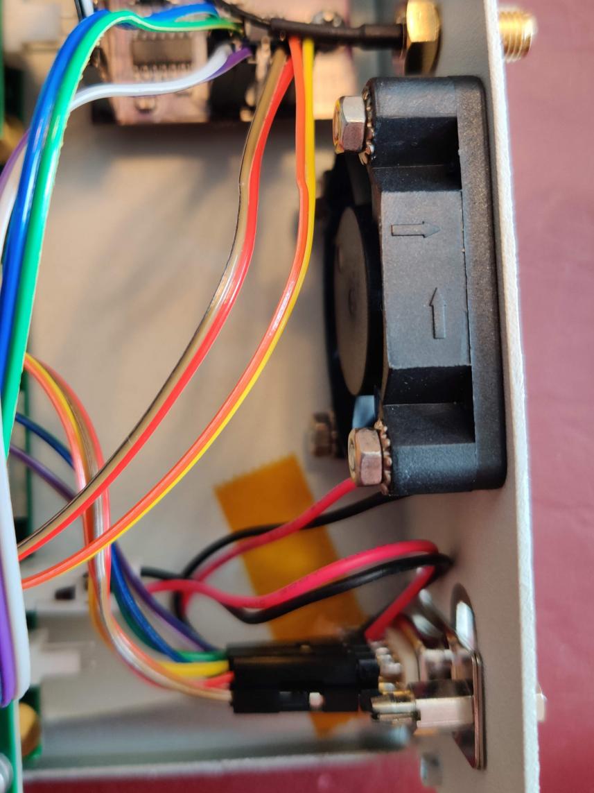
Install the fan, making sure to re-install it the same way it was originally installed.
Pre-Assemble the TXIO board before installation into the N200
Begin by connecting eight 0.1” female-female jumper cables to pins 1-4 and 6-9 of the D-sub connector. The other ends of these wires connects to header J2 on the TXIO board
J2 Pin
Pin label
Wire colour
DSUB Pin
1
LP-
Grey
4
2
TM-
Blue
3
3
LP+
Purple
9
4
TM+
Green
8
5
GND
[NC]
[NC]
6
GND
[NC]
[NC]
7
AGC-
Brown
1
8
TR-
Orange
2
9
AGC+
Red
6
10
TR+
Yellow
7
[NC]
[NC]
[NC]
5
Connect the four U.Fl to SMA female bulkhead cables to J4, J5, J6 and J7 of the TXIO board. Orientation of the cables doesn’t matter, as they will fit in the N200 case if rotated properly.
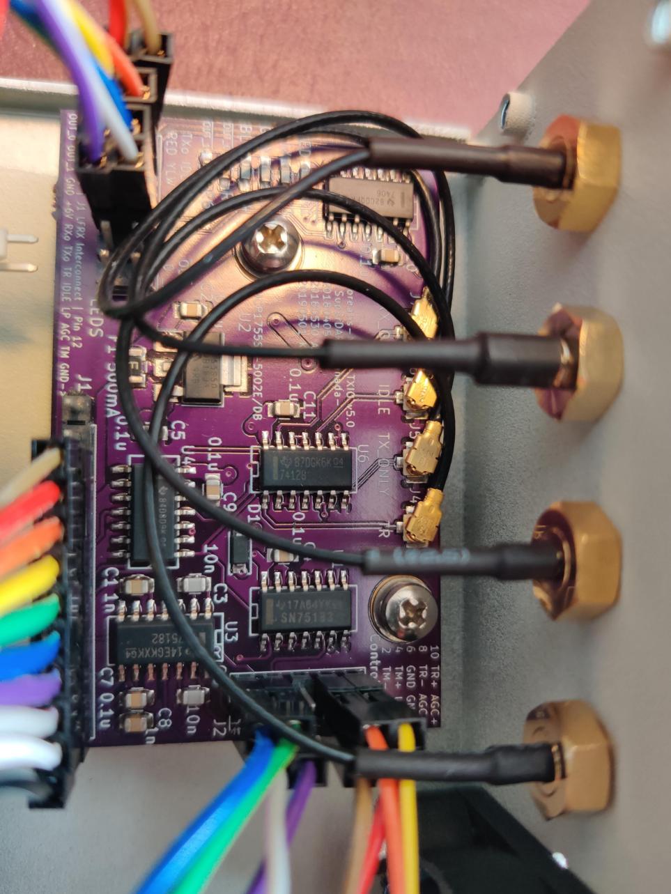
Connect 4 pairs of 0.1” female to female jumper wires to header J3 on the TXIO board. THe other ends will connect to the LEDs already installed in the N200 case. There is no need to connect anything to the 4 rightmost pins on J3, these are expansion headers and two are connected (label ‘OUT’) to the leftover open collector pins on the LED driver chip U5 (SN7406D), the other two (labels ‘_0’ and ‘_1’) are connected to the 5V rail via pullup resistors R5 and R6.
Note
If you use your own voltage supply with the open-collector outputs, be aware that the maximum voltage is 30V, and the maximum current sink is 40mA. See the SN7406D datasheet for more details.
J3 Pin label
Wire Colour
LED Connection
TXo
Brown
RED-
RED
Red
RED+
IDLE
Orange
Yellow-
YLW
Yellow
Yellow+
RX
Blue
Green-
GRN
Green
Green+
TX
Grey
Blue-
BLU
Purple
Blue+
Note
‘-’ means cathode, ‘+’ means anode
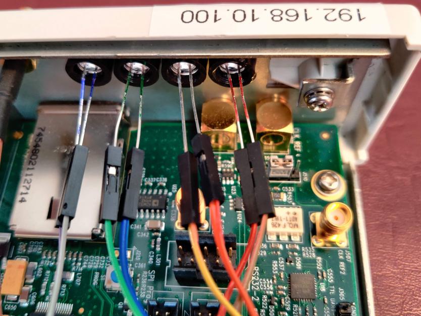
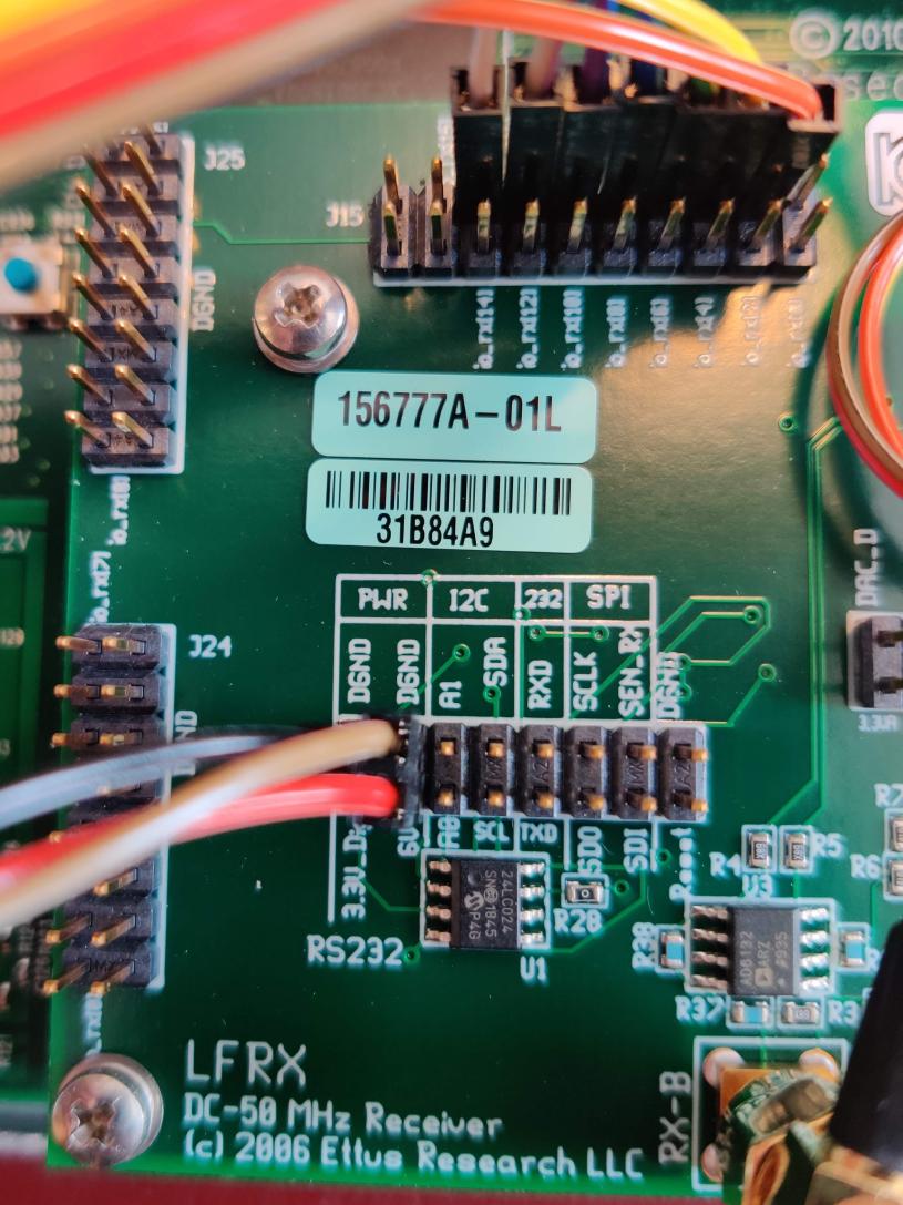
Connect 10 0.1” female to female jumper wires to J1, the other ends will connect to the LFRX daughterboard pin headers.
J1 Pin
Pin label
Wire colour
LFRX header
LFRX Pin
1
OUT_0
[NC]
[NC]
[NC]
2
OUT_1
[NC]
[NC]
[NC]
3
GND
Brown
J16
‘DGND’
4
+6V
Red
J16
‘6V’
5
RXo
Orange
J15
io_rx[1]
6
Txo
Yellow
J15
io_rx[3]
7
TR
Green
J15
io_rx[5]
8
IDLE
Blue
J15
io_rx[7]
9
LP
Purple
J15
io_rx[9]
10
AGC
Grey
J15
io_rx[11]
11
TM
White
J15
io_rx[13]
12
GND
Black
J16
‘DGND’
Install the TXIO board by screwing it into place on the USRP housing with the two provided holes. The TXIO board uses the same size and style of screw that the N200 motherboard and daughtercards do.
Install the DSUB connector with the provided standoff screws.
Note
Some models of DSUB will have split lock washers, but we’ve found that the thickness of the N200 case is too thick to use them. The DSUB standoff screws are notoriously easy to snap as well, so be careful.
Install the 4x SMA female bulkhead cables at the back of the N200, when facing the rear of the N200 case the order from left to right is: J4, J5, J6, J7 (the same order as on the PCB, so no wires should cross each-other).
Finally, connect the LFRX jumper wires from J1 and LED wires from J3 to complete the installation.
Configuring the Unit for Borealis
Use UHD utility
usrp_burn_mb_eepromto assign a unique IP address for the unit. Label the unit with the device IP address:cd <install path>/lib/uhd/utils ./usrp_burn_mb_eeprom --args="addr=<current ip> --values="ip_addr=<new ip>"
Note
Recommended IP addresses are
192.168.10.100-116for the N200s (116 is the spare),192.168.10.130-132for the octoclocks (.131is for the GPS octoclock), then192.168.10.60for the borealis computer’s 10G interface (or some other IP address in the same192.168.10.Xsubnet that is above192.168.10.3, which is the default for octoclocks from the factory.The device should be configured and ready for use.
Pre-amps
For easy debugging, pre-amps are recommended to be installed inside existing SuperDARN transmitters where possible for SuperDARN main array channels. SuperDARN transmitters typically have a 15V supply and the low-noise amplifiers selected for pre-amplification (Mini-Circuits ZFL-500LN) operate at 15V, with max 60mA draw. The cable from the LPTR (low power transmit/receive) switch to the bulkhead on the transmitter can be replaced with a couple of cables to and from a filter and pre-amp.
Note
Existing channel filters (typically custom 8-20MHz filters) should be placed ahead of the pre-amps in the RF path to avoid amplifying noise.
It is also recommended to install all channels the same for all main array channels to avoid varying electrical path lengths in the array which will affect beamformed data.
Interferometer channels will need to be routed to a separate plate and supplied with 15V by a separate supply capable of supplying the required amperage for a minimum of 4 pre-amps.
Control Computer
Borealis requires a high-performance computer to operate. See Borealis Control Computer for the full computer specifications. Follow the manuals for the motherboard purchased to assemble the computer. Notes on building a Borealis computer:
Update the BIOS when working with a new motherboard
XMP must be enabled in BIOS to utilize the full 6000 MHz RAM speed. RAM must also be socketed in the optimal configuration DIMM_A2 and DIMM_B2 for two sticks.
CPU cooling is crucial. Borealis will run many cores at its maximum, generating significant heat.
PCIe ports must be dedicated to single devices, and not split between components. Proper operation requires maximized PCIe bandwidth.
Octoclocks and Networking
One issue with the Octoclock units is that they contain a very basic Ethernet controller chip, the ENC28J60. This means that the Octoclock units will only operate at 10Mbps link speed (10BASE-T). The previously used 10Gb network switches (NetGear XS708E-200NES or XS708T) only operated at 100Mbps, 1000Mbps and 10000Mbps. Therefore, a 5-port unmanaged switch was required to connect all three Octoclocks to one of the 10Gbps network switches. The 5-port switch had to be capable of operating at both 10Mbps and 100Mbps so it could connect to both the Octoclocks as well as the XS708E switch. The network cables connecting the Octoclocks to the 5-port switch do not need to be dual shielded and any Cat5 cable (or better) should work.
NTP discipline with PPS (Optional)
Some aspects of Borealis depend upon the operating system having the correct time. The Network Time Protocol (NTP) can be used to provide a stable and accurate system clock. A correct system clock, along with proper programming, can help to catch GPS issues and make sure that the Borealis scheduler starts and stops control programs as close as possible to the correct time.
Though not strictly necessary for the Borealis radar to operate, a more stable and accurate clock can be achieved by disciplining NTP with a Pulse-Per-Second (PPS) signal. There are several unused outputs on the Octoclock-g clock distribution unit. An unused PPS signal can be used from the Octoclock-g to help NTP discipline the Borealis computer’s onboard clock. In ideal conditions, with PPS disciplined NTP running, the Borealis computers at several SuperDARN Canada sites are disciplined to within a few microseconds of UTC time. This is several orders of magnitude better than without a PPS signal.
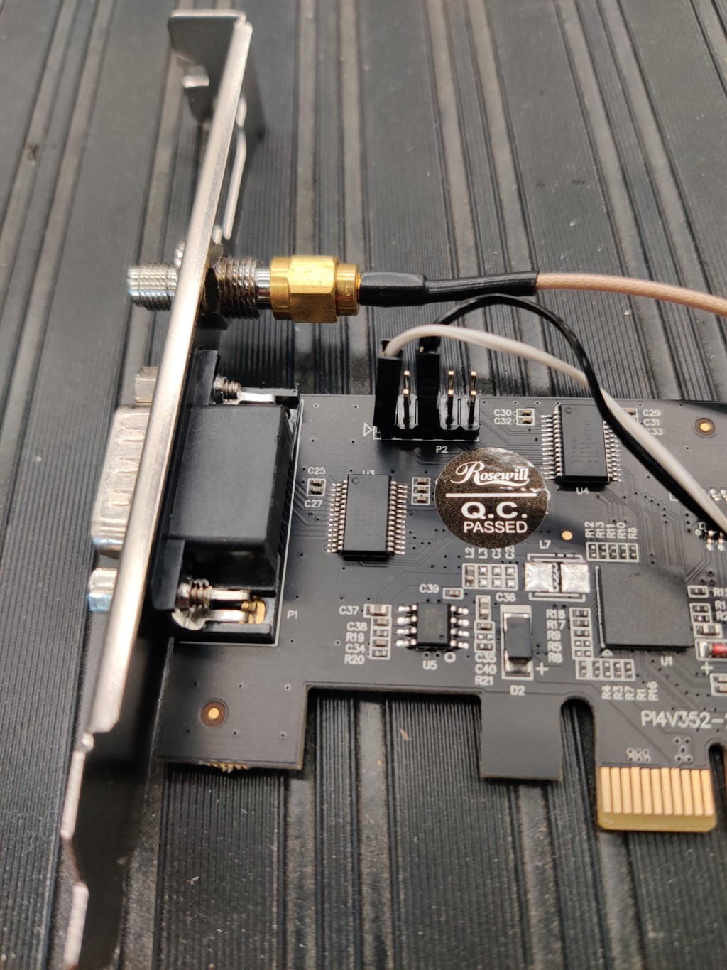
To utilize this ability of NTP, a coaxial cable needs to be modified so that one end connects to the DCD and GND pins of the motherboard’s COM port. In addition to creating the cable and connecting it to the appropriate pins, see the next section’s NTP setup guide to properly set up the software to handle the incoming PPS signal.
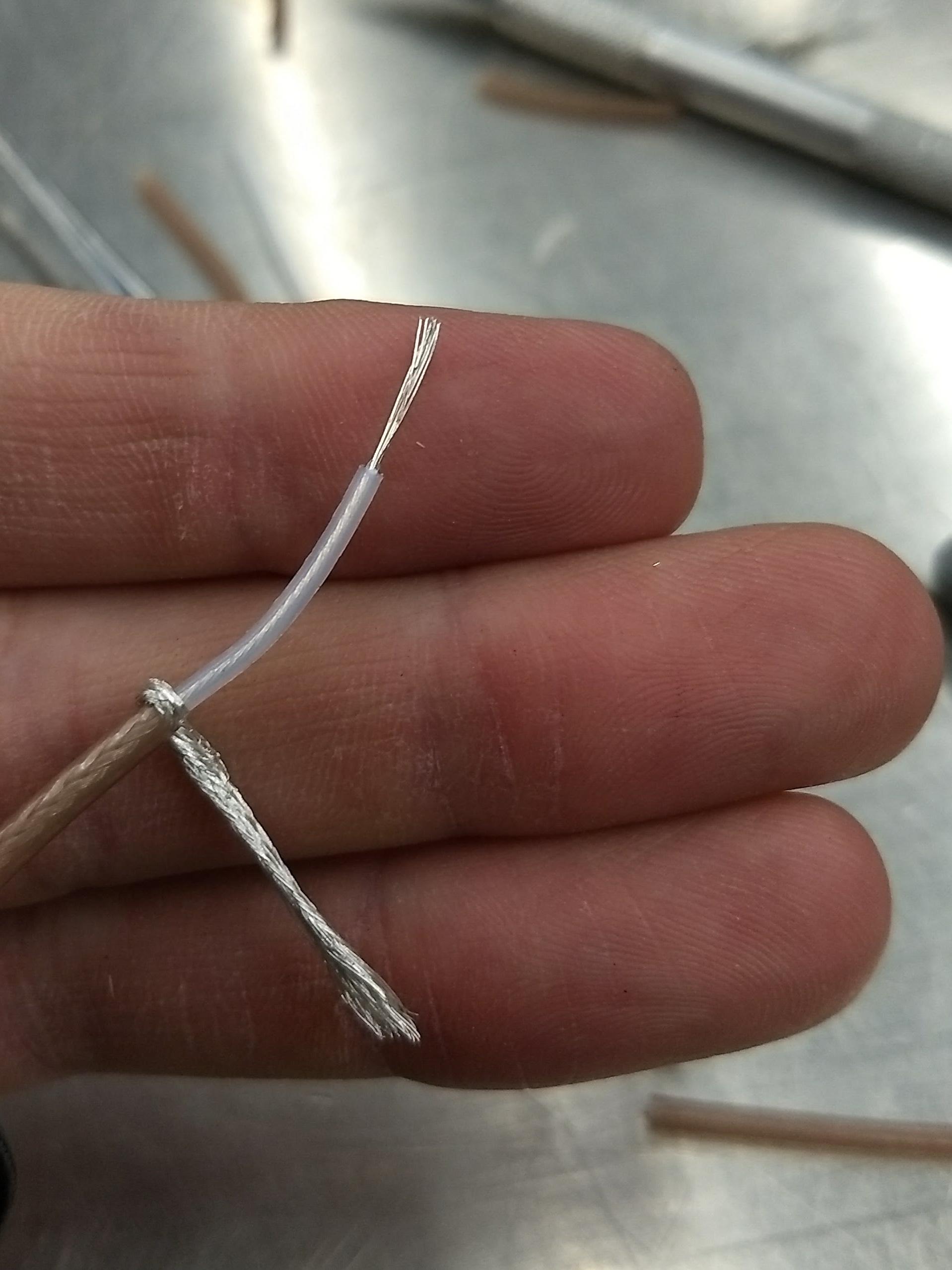
The photo below shows how the center conductor and shield of a coaxial cable are stripped, so they can be soldered to hookup wire to connect to the header pins on the motherboard COM port. The other end of the coaxial cable is connected to one of the PPS outputs of the Octoclock-g clock distribution unit.
The COM ports on off-the-shelf motherboards are typically 0.1” spaced header pins, in a shrouded connector. This means that you can use one of the 0.1” female-female jumper cables from the N200 assembly steps, cut it in half and solder the bare wire end to the coaxial cable stripped wire ends.
Note
The centre conductor is attached to the DCD pin and the braid is connected to the GND pin.
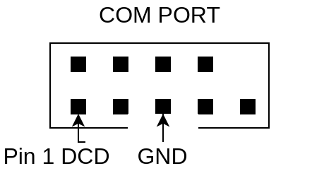
A typical pinout for COM ports is shown below, but check with your motherboard’s user manual to verify both the location and pinout:
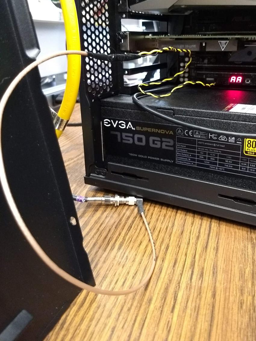
The photo below shows the modified coaxial cable in place. On the motherboard version in the photo, the onboard COM port is to the left of the ‘AA’ shown on the 7-segment display.
In case your motherboard does not have a COM port routed out to a pin header, you can purchase and use a PCIe serial port card. One such part that is known to work is the Rosewill RC-301EU. The photo below shows how one of these cards was modified by removing the physical D-Sub connector and using a bulkhead SMA connector in place.